
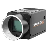
 MV-CS050-10GM(NPOE)View part & specifications →Browse camera options →
Inicio / Case studies / LED-panel and substrate appearance
Application study · Electronic component manufacturingLED panels and substrates: reveal the repeated pattern without implying electrical performance
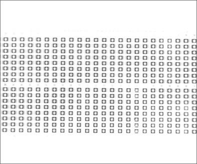
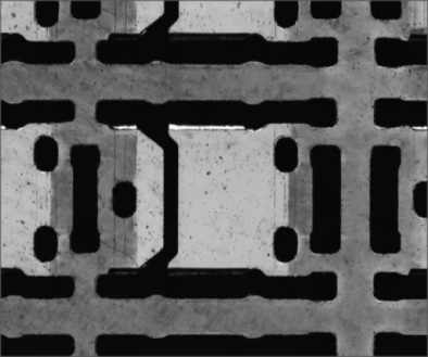
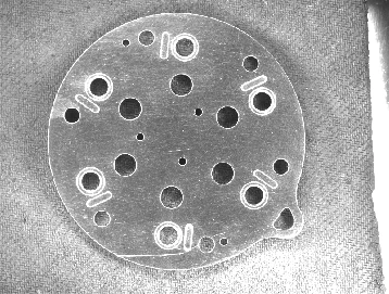
Two independent source captures show a dense lamp-panel array and a larger substrate pattern. Flat coaxial lighting makes the repeated geometry visible for an appearance trial; the images do not establish whether the devices light or conduct correctly.
Use the pattern for appearance checks and verify device function independently.
- Light in sourceLS-FCS100 · white
- EvidenceReal application-lab image
- Imaging kitCamera, lens and fixture proposed
- AcceptanceValidate on representative parts
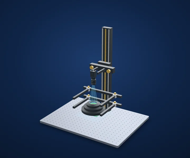
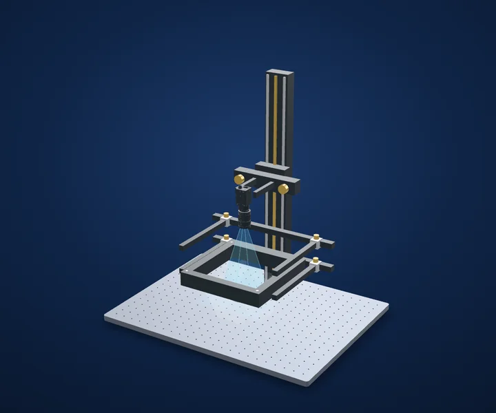
Test stationIncluded light holdersCámaraLenteLuzPartCampo de visión
 Drag to rotate · scroll to zoom
Walk through this setup 5 guided stops
From component to inspection
Understand each choice.
Choose a stop to frame the part in 3D and see why it belongs in this setup. The component notes and links remain available if 3D cannot load.
Proposed component
MV-CS050-10GM(NPOE)
5 MP monochrome global-shutter camera proposed for a contrast trial. Confirm field, sampling, exposure and algorithm on the actual application.
Proposed component
LS-KF1628M-ML
Proposed 16 mm C-mount macro lens at its printed 0.1x magnification / 152 mm working-distance pair. The proposed 2448 × 2048 sensor with 3.45 µm pixels gives a derived 84.456 × 70.656 mm field; confirm focus, coverage and residual distortion on the real sample.
Tested component
LS-FCS100
White LS-FCS100 identified in the lamp-panel source capture. The separate substrate example names white LS-FCS200, shown as an alternative and excluded from this proposed kit.
Proposed component
LS-BT-XZ-G-6-6045
600 mm column, 600 × 450 mm breadboard, XZ adjustment, glass tray and two lighting holders as listed. Proposed bench fixture; confirm loads, travel and camera/lens clamps.
Inspect the real capture
Follow the contrast to the part.
Use the pattern for appearance checks and verify device function independently.
Camera and available lens CAD are published models. Lens and light envelopes use printed dimensions. The linked station uses its published base size and column height; carriage, brackets, fittings, parts and spacing are illustrative. Confirm load, travel, fasteners and clearances before ordering. Light paths explain the arrangement and do not simulate optical performance. Representative part geometry is illustrative, not reconstructed inspection evidence. The specimen and lighting angle are representative, not dimensions or settings recovered from the source capture.
From the demo to your test benchCámaraMV-CS050-10GM(NPOE)View part & specifications →Browse camera options → Imaging lens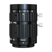 LS-KF1628M-MLView part & specifications →Browse imaging lens options →
Inspection light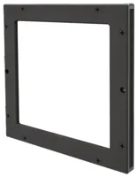 LS-FCS100View part & specifications →Browse inspection light options →
Test station & mounts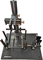 LS-BT-XZ-G-6-6045View part & specifications →Browse test station & mounts options →
Build around the parts you can buy.
Explore each component, check its specifications and compare alternatives. The proposed quote includes the linked test station; its catalog listing includes two lighting holders.
MV-CS050-10GM(NPOE)View part & specifications →Browse camera options →LS-KF1628M-MLView part & specifications →Browse imaging lens options →LS-FCS100View part & specifications →Browse inspection light options →LS-BT-XZ-G-6-6045View part & specifications →Browse test station & mounts options →Mount the optics with intent
The station is an optical test bench, with its two lighting holders included in the catalog listing. The 3D column and base follow the published height and footprint. Carriages, clamps and part supports are schematic: confirm camera screw pattern, lens support, light fasteners, permissible load and actual travel before ordering.
Configure the mounting station →Complete the electrical system
Select a controller against the exact light voltage, drive mode and power, then confirm camera data/power/I/O cables and a suitable PC. These are not silently added to the proposed optical kit.
Lighting application-lab catalog capture
Evidence you can inspect
Visible in the images
The lamp-panel array and the separate patterned substrate have visible repeated geometry.
What the source reports
The source labels lamp-panel and LED-substrate defect inspection and identifies their respective white flat coaxial lights.
How to use this evidence
Two different source samples, without labelled individual defects, minimum feature size, detection results or device-function data.
What the camera saw
Cropped from the source test sheet; original test annotations are retained. Captures are not generated or enhanced. Drag the comparison slider or use the image buttons.
The challenge
A large repeated array can hide local missing or malformed features in otherwise similar neighbours.
Surface marks and pattern geometry must be distinguished from actual electrical defects.
How it was solved
The catalog identifies a white 100 mm flat coaxial light for the lamp-panel example and a white 200 mm version for the independent substrate example.
Choose a proposed field that resolves the required repeated feature. The illustrated panel is representative and does not recreate either source sample or prove whole-panel coverage.
Why it works
- 1
A broad light-guide arrangement provides a reflected view of repeated features with a compact light envelope.
- 2
The observed patterns support visual inspection planning, but the source images are not electrical or optical-output tests.
From image contrast to a production decision
What to validate on your part
A useful sample image is the starting point. These are the checks that turn the concept into a defensible inspection.
- 01
Define the visible defect classes
Include missing, displaced and damaged features as well as accepted pattern variation.
- 02
Check the entire planned field
Confirm focus and sampling at corners and centre without inferring the source part scale.
- 03
Retain functional testing
Validate electrical continuity or emitted-light performance separately when required.
Explore your inspection requirementsNo limit from motion
How many pixels cover your feature?
Compare feature coverage, camera pixel requirements and exposure using your own planning inputs. These are calculated planning values, not inspection results or an accuracy specification.
Editable planning scenario. Adjust these example inputs for your application; they are separate from the source test and 3D setup. Motion allowance and target coverage are starting points to validate, not acceptance limits. Pixel count starts from the proposed camera's catalog resolution.
Enter finite numbers in every field. Field width, feature width, target coverage, exposure and allowed motion must be greater than zero; horizontal pixel count must be a positive whole number; material speed may be zero. Use values within the supported numeric range if a calculation cannot be represented.
Object sampling mm/px
Pixels across feature px
Horizontal pixels for target px
Motion during exposure px
Exposure ceiling from motion µs
Formulas and assumptions
The field, feature, speed and exposure start with neutral example values. They are not taken from the source test or the 3D illustration. Allowed motion starts at an editable 0.5-pixel example; it is not a recommended acceptance limit. Target coverage starts at an editable 5-pixel example; it is not a recommended detection or measurement threshold. The horizontal pixel count starts from the catalog Resolution row for MV-CS050-10GM(NPOE). Use the effective width after cropping, binning or decimation if those modes are enabled.
- Object sampling (mm/px) = field width (mm) / horizontal pixels.
- Pixels across feature = feature width (mm) / object sampling (mm/px).
- Horizontal pixels for target = field width (mm) × target pixels across feature / feature width (mm), rounded up to a whole pixel.
- Motion (px) = speed (mm/s) × exposure (µs) / 1,000,000 / object sampling (mm/px).
- Exposure for allowed motion (µs) = allowed motion (px) × object sampling (mm/px) / speed (mm/s) × 1,000,000.
The exposure result is the maximum duration from this motion allowance alone. At zero speed, motion sets no exposure limit; the camera, lighting, saturation and other constraints still apply. A shorter exposure does not itself guarantee a reliable inspection.
Field width and feature width refer to the same object plane. The motion calculation assumes uniform linear motion parallel to the field-width direction and a single exposure. It does not model perspective, vibration, rolling-shutter distortion, diffraction, defocus or optical distortion. A strobe may change the effective exposure.
The target result is a horizontal sampling requirement, not a camera recommendation or a change to the selected camera. It uses the effective image width after cropping, binning or decimation and does not determine the vertical resolution or sensor size. Pixel coverage alone does not establish detectability or measurement accuracy. Validate contrast, lens performance, working distance, illumination, calibration, camera exposure limits and the inspection algorithm on representative parts. Changing field width does not change the 3D model or certify that the proposed lens can achieve that field.
The set-up and the parts
| Tested light | LS-FCS100, white |
|---|---|
| Source camera / lens | Not specified in the source image caption; proposed parts below |
| Proposed lens point | 0.1x at 152 mm, printed lens pair |
| Derived proposed field | 84.456 × 70.656 mm = sensor dimensions / 0.1x; not a source test field |
| Primary light-guide area | 100 × 100 mm, printed |
| Primary housing | 140 × 140 × 10 mm, printed |
| Separate source alternative | LS-FCS200, white, 200 × 200 mm light-guide area |
| Mounting (proposed) | LS-BT-XZ-G-6-6045; 600 mm column, 600 × 450 mm base, glass tray and two included lighting holders |
LuzTestedLS-FCS100
White LS-FCS100 identified in the lamp-panel source capture. The separate substrate example names white LS-FCS200, shown as an alternative and excluded from this proposed kit.
$289.00In proposed setupSeparate substrate-test alternativeTestedLS-FCS200
White version identified in the independent LED-substrate capture; printed 200 × 200 mm light-guide area and 240 × 240 × 10 mm housing. Different sample and recipe, excluded from this proposed kit.
$789.00Separate test / alternativeCámaraOur pickMV-CS050-10GM(NPOE)
5 MP monochrome global-shutter camera proposed for a contrast trial. Confirm field, sampling, exposure and algorithm on the actual application.
$819.00In proposed setupLenteOur pickLS-KF1628M-ML
Proposed 16 mm C-mount macro lens at its printed 0.1x magnification / 152 mm working-distance pair. The proposed 2448 × 2048 sensor with 3.45 µm pixels gives a derived 84.456 × 70.656 mm field; confirm focus, coverage and residual distortion on the real sample.
$319.00In proposed setupCamera test stationOur pickLS-BT-XZ-G-6-6045
600 mm column, 600 × 450 mm breadboard, XZ adjustment, glass tray and two lighting holders as listed. Proposed bench fixture; confirm loads, travel and camera/lens clamps.
$359.00In proposed setup"Tested" identifies the part named in the source. "Our pick" is a proposed alternative or supporting part. The quote includes only cards marked "In proposed setup", with the quantities shown; other test arrangements are separate. Confirm colour, optics, controllers, power supplies, cables and mounting before ordering.
About this case study: the photos and camera images come from the application laboratory of the maker of the lighting and optics we sell, imaged on the parts shown; your results depend on your part, camera and set-up. This is an application-lab study, not a LumaSpec customer deployment. Source figures are reported results; proposed components require a fresh trial. The 3D scene illustrates the arrangement and does not simulate imaging performance.
More case studies
Lithium battery manufacturing · Surface defect detection
Battery welds and tabs
Control what shiny metal reflects.
- LuzFlat dome, 100 × 100 mm emitting
- Tamaño140 × 140 × 11.5 mm
Electronics (SMT / AOI) · Solder joint inspection
PCB solder joints with an RGB AOI light
Use lighting angle to make solder shape visible.
- LuzAOI, 160 mm outside, 45 mm aperture
- Altura55 mm
Precision machining · Surface defect detection
Scratches on machined metal
Choose lighting direction before adding resolution.
- Test lightFour-sided adjustable bar light
- Housing (spec)230 × 230 × 37 mm
Start with your inspection requirement
Make the next trial specific.
Tell us the part size, smallest defect or tolerance, available working distance, material and line speed. Include what a good part and a reject look like.
Discuss your applicationConfigurar un sistema